
Every Stage of Optical Device Production
With its world-beating line of optical devices, including semiconductor pumping lasers for long-distance optical-communications applications, gain chips and semiconductor amplifiers supporting data communications, power supplies for gas-sensing, etc., every product from Anritsu Devices*1 is fabricated with a focus on lower prices, faster speeds, and higher stability.
This presentation puts the spotlight on these optical-device fabrication processes.
*1: Name of our device-fabrication company
Our composite semiconductor devices based on either indium phosphide (InP) or gallium arsenide (GaAs) substrates are fabricated in a 2500-m2 cleanroom specializing in optical devices. All processes ranging from upstream wafer growth to device assembly, packaging, inspection, and shipping are handled in the same building to maintain smooth production featuring excellent communications and meeting customers’ requirements.
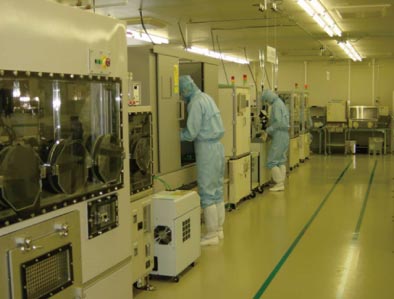
Fig. 1 Clean Room for Manufacturing Optical Devices
Outline of Manufacturing Process
1. Wafer Growth ~ Electrode Forming
The high-purity epitaxial crystal is grown using a MOVPE (metalorganic vapor-phase epitaxy) reactor to form a compound multilayered semiconductor structure based on the theoretical design. These compound multilayers form the basis of the high stability of our various high-performance optical devices.

Fig. 2 Outline of Wafer Processing
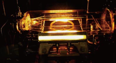
Fig. 3 MOVPE Reactor Tube
2. Chipping ~ Chip Assembly
In this process, the wafer is cut into bars and cleaved to create the resonator structure required for laser oscillation; the facets are coated to adjust the reflectance and form a protective coating. Then the bars are separated into individual chips (Fig. 5) before testing with a dedicated chip tester (Fig. 6) to assure that only good chips meeting all the required static characteristics, such as output power, are selected by the automatic chip picker.

Fig. 4 Outline of Chipping
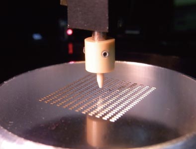
Fig. 5 Dividing Chips
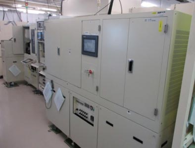
Fig. 6 Chip Tester
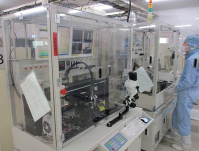
Fig. 7 Automatic Bonding Machines
At assembly, the automatic die bonder (Fig. 7 left) and automatic wire bonder (Fig. 7 right) perform assembly with a high positional stability of 4 μm.
All finished products are subjected to aging tests to assure reliability by removing products with poor performance right from the start. At the final stage, products are subject to automated characteristics tests before passing to the module assembly process.
3. Module Assembly
To assure stable quality and low cost, our modules adopt a design platform using common parts. A scalar robot with various rotational axes performs automated assembly of the laser diode, photodiode, etc., on the board using a chip carrier and PD automatic assembler (Fig. 9 left). Next, the Peltier element is assembled in the module by the automatic Peltier element and board loader. The lens and isolator are assembled by the lens alignment fixer (Fig. 10) before packaging in dry nitrogen gas and seam welding.
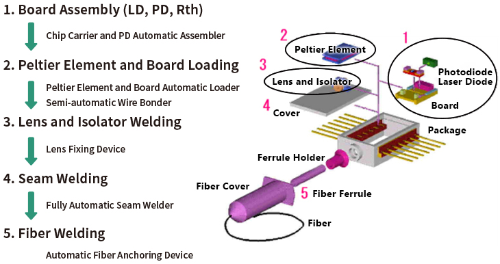
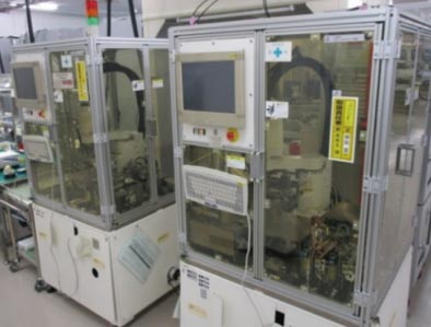
Fig. 9 Automatic Peltier Element and Board Loader
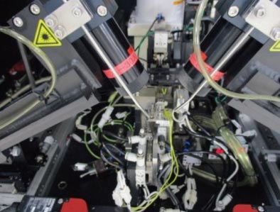
Fig. 10 Automatic Lens Alignment System (internal)
At the final stage, the lens alignment system (Fig. 11) uses high-coupling efficiency YAG laser welding to align the optical fiber before fitting the covers.
After aligning the optical fiber, a constant- temperature chamber and thermal-shock chamber are used to check there is no stress relaxation and joint abnormality. Following confirmation of a stable output, etc., the part is sent to the final inspection stage.
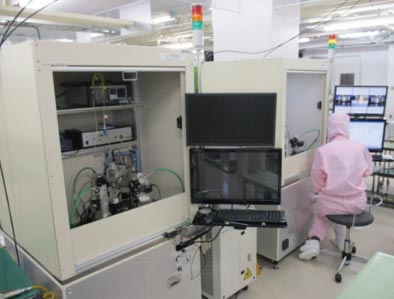
Fig. 11 Automatic Lens Alignment System
4. Inspection
The characteristics and quality of assembled completed modules are confirmed by the inspection process.
An aging jig (Fig. 12) running continuous energization tests is used to confirm that there are no hidden problems in the processes. Additionally, a dedicated automatic characteristics tester (Fig. 13) examines the main characteristics, such as the optical output, optical spectrum, etc., before shipping products passing these final tests to customers.
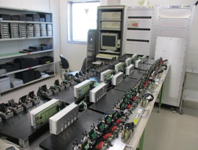
Fig. 12 Aging Jig (Device)
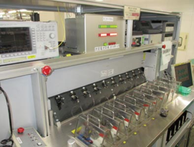
Fig. 13 Automatic Characteristics Tester
5. Evaluation Equipment
To maintain the highest reliability, we focus heavily on product quality control using various equipment for testing and evaluation, such as a scanning electron microscope and X-ray analysis equipment, as well as die shear tester, wire-pull tester, and gross- and fine-leak testers to confirm bonding quality. A tension tester evaluates weld bond strength and a thermal shock tester (Fig. 14) evaluates environmental durability. Any voids in solder joints are discovered using an ultrasound microscope (Fig. 15).
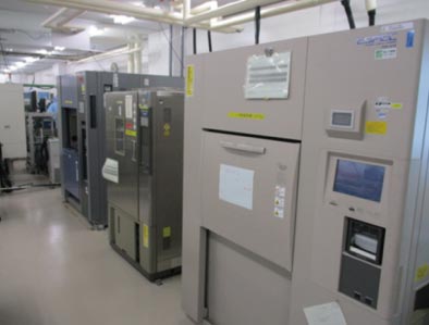
Fig. 14 Thermal Shock Tester, etc.
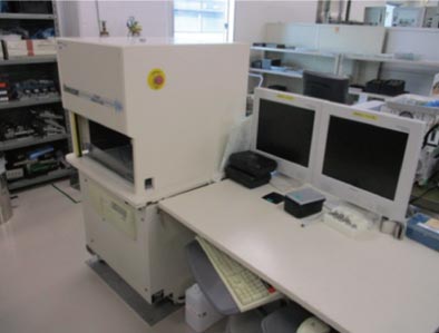
Fig. 15 Ultrasound Microscope (Bonding Evaluation)
Optical Sensing for Industry >
Optical Sensing for Medicine >
Optical Devices for Communication >